

Click to open expanded view
HC-DSL09S0P1T2 136–941 MHz, 0.15W, 3.7 V BroadBand RF Power Transistor
N-Channel Enhancement-Mode MOSFET
Designed for handheld two–way radio applications with frequencies from 136 to 941 MHz. The high gain, ruggedness and Broadband performance of this device make it ideal for large–signal, common–source amplifier applications in handheld radio equipment.
Typical Broadband EVB Performance (IDQ=90mA, TA = 25℃, CW)
|
VDS |
Freq. |
Gmax |
Pout |
PAE |
|
|
[V] |
[MHz] |
[dB] |
[dBm] |
[mW] |
[%] |
|
3.7 |
400 |
17.5 |
22.0 |
160 |
53.4 |
|
440 |
16.0 |
23.2 |
210 |
67.4 |
|
|
480 |
15.4 |
23.2 |
210 |
64.4 |
|
|
520 |
13.8 |
23.0 |
200 |
61.3 |
|
Ÿ Capable of Handling 20:1 VSWR @ 6.0 Vdc, 0.2 Watts, CW
Features
Ÿ Characterized for Operation from 136 to 941 MHz
Ÿ Unmatched Input and Output Allowing Broad Frequency Range Utilization
Ÿ Integrated ESD Protection
Ÿ Broadband – Full Power Across the Band
Ÿ Exceptional Thermal Performance
Ÿ Extreme Ruggedness
Typical Applications
Ÿ Output Stage VHF Band Handheld Radio
Ÿ Output Stage UHF Band Handheld Radio
Ÿ Output Stage for 700–800 MHz Handheld Radio
Ÿ Driver for 10–1000 MHz Applications
Table1. Maximum Ratings
|
Rating |
Symbol |
Value |
Unit |
|
Drain-Source Voltage |
VDSS |
–0.5, +20 |
Vdc |
|
Gate-Source Voltage |
VGS |
–0.5, +8 |
Vdc |
|
Operating Voltage |
VDD |
0, +6 |
Vdc |
|
Storage Temperature Range |
Tstg |
–65 to +150 |
℃ |
|
Case Operating Temperature |
TC |
–40 to +150 |
℃ |
|
Operating Junction Temperature |
TJ |
–40 to +150 |
℃ |
|
Power Dissipation @TC=25℃ |
PD |
0.25 |
Watts |
Table 2. ESD Protection Characteristic
|
Test Methodology |
Class |
|
Human Body Model (per JESD22--A114) |
2, passes 2500 V |
|
Machine Model (per EIA/JESD22--A115) |
A, passes 100 V |
|
Charge Device Model (per JESD22--C101) |
IV, passes 2000 V |
Table 3. Electrical Characteristics (TA=25℃ unless otherwise noted)
|
Characteristic |
Symbol |
Min |
Typ. |
Max |
Unit |
Off Characteristics
|
Gate-Source Leakage Current (VGS=5Vdc, VDS=0Vdc) |
IGSS |
- |
- |
500 |
nAdc |
|
Zero Gate Voltage Drain Leakage Current (VDS=16Vdc, VGS=0Vdc) |
IDSS |
- |
- |
100 |
nAdc |
|
Zero Gate Voltage Drain Leakage Current (VDS=3.7Vdc, VGS=0Vdc) |
IDSS |
- |
- |
100 |
nAdc |
On Characteristics
|
Gate Threshold Voltage (VDS=3.7Vdc, ID=1mA) |
VGS(th) |
1.6 |
1.8 |
2.0 |
Vdc |
|
Gate Quiescent Voltage (VDD=3.7Vdc, ID=90mA Measured in Functional Test) |
VGS(Q) |
2.2 |
2.6 |
2.8 |
Vdc |
|
Drain-Source On-Voltage (VGS=5Vdc, ID=100mA) |
VDS(ON) |
- |
0.28 |
- |
Vdc |
Dynamic Characteristics
|
Reverse Transfer Capacitance (VDG=3.7V, Level=30mVac@1MHz) |
Crss |
- |
0.25 |
- |
pF |
|
Output Capacitance (VDS=3.7V, Level=30mVac@1MHz) |
Coss |
- |
1.8 |
- |
pF |
|
Input Capacitance (VGS=5V, Level=30mVac@1MHz) |
Ciss |
- |
8.0 |
- |
pF |
Typical Performances (In DuSemi Narrowband Test DEMO,50 Ohm system)
Frequency=440MHz, VDD=3.7Vdc, ID(Q)=90mA, Pin=7dBm, TA=25℃
|
Output Power |
Pout |
- |
151 |
- |
mW |
|
Power Gain |
GPS |
- |
15 |
- |
dB |
|
Drain Efficiency
|
ηD |
- |
50 |
- |
% |
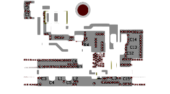
Broad Band Evaluation Circuit (@VDD = 3.7V, f = 440 MHz)
![]()
Table 5. Test Circuit Component Designations and Value
|
Part |
Description |
Part Number |
Manufacturer |
|
R3 |
470Ohm |
— |
— |
|
R4 |
6.8KOhm |
— |
— |
|
L1, L2 |
4.7nH |
— |
— |
|
L3 |
8 Turns D: 0.5 mm, φ 2.4 mm Enamel Wire |
— |
— |
|
C3,C15, |
100pF Chip Capacitors |
GQM21P5C1H101JB01 |
Murata |
|
C4 |
18pF Chip Capacitors |
GRM1885C1H201JA01 |
Murata |
|
C12, C9 |
1000pF Chip Capacitors |
GRM1885C1H102JA01 |
Murata |
|
C10, C14,C7 |
10uF,25VChip Capacitors |
— |
— |
|
C5 |
24pF Chip Capacitors |
— |
Murata |
|
R1,R2,C1,C2,C8,C6 |
NC |
— |
— |
|
U1 |
LM1117 |
||
|
PCB |
FR-4 ,1.6mm, Ɛr4.5 |
— |
Если вам нужна дополнительная информация, пожалуйста, свяжитесь с нами.
