Click to open expanded view
HC-DSV136N 15W silicon RF-MOS power transistor
Product profile
General description
A 15 W silicon RF-MOS power transistor for broadcast applications and industrial applications in the HF and VHF band. Designed primarily for wideband large-signal output to 400MHz.
Table 1. Production test information
|
Mode of operation |
F (MHz) |
VDD(V) |
PL(W) |
Gp(dB) |
ηD(%) |
|
CW |
150 |
28 |
27 |
21 |
78 |
Features
u Common source configuration
u Typical CW performance @ Freq=150MHz,VDD= 28Vdc , IDQ=100mA
Average output power = 25 W
Power gain = 21 dB
Efficiency = 78 %
u Excellent thermal stability
u Excellent ruggedness
u High power gain
u High efficiency
u 10:1 VSWR capability
u Easy power control
Application
Industrial, scientific and medical applications
Broadcast transmitter applications
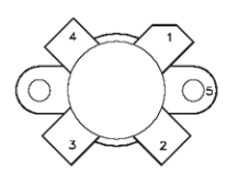
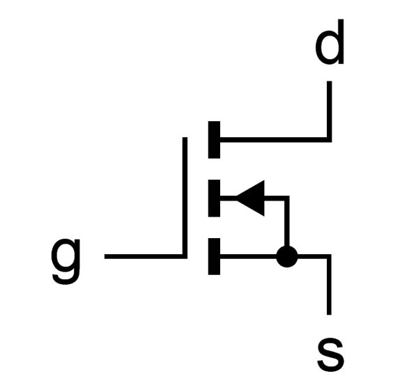
Pinning information
Table 2.Pinning
|
Pin |
Description |
Simplified outline |
Graphic symbol |
|
1 |
Drain |
|
|
|
3 |
Gate |
||
|
2、4、5 |
Source(Flange) |
Limiting values
Table 3.Limiting values
|
Symbol |
Rating |
Values |
Unit |
|
VDSS |
drain-source voltage |
90 |
V |
|
VGS |
gate-source voltage |
±30 |
V |
|
ID |
drain current |
5 |
A |
|
Tstg |
storage temperature |
-65 to +150 |
℃ |
|
Tj |
junction temperature |
200 |
℃ |
Thermal characteristics
Table 4.Thermal characteristics
|
Symbol |
Parameter Typ. Unit |
|
|
Rth(j-c) |
thermal resistance from junction to case 2.6 ℃/W |
Characteristics
Table 5. DC characteristics
Tj = 25℃ unless otherwise specified.
|
Symbol |
Parameter |
Conditions |
Min |
Typ |
Max |
Unit |
|
V(BR)DSS |
drain-source breakdown voltage |
VGS = 0 V; ID = 1 mA |
75 |
- |
- |
V |
|
VGS(th) |
gate-source threshold voltage |
VDS = 10 V; ID =50 mA |
1.0 |
2.7 |
5.0 |
V |
|
IDSS |
drain leakage current |
VGS = 0 V; VDS =28 V |
- |
- |
10 |
uA |
|
IGSS |
gate leakage current |
VGS = ±30 V; VDS = 0 V |
- |
- |
±1 |
uA |
|
gfs |
forward transconductance |
VDS = 10 V; ID = 3 A |
0.8 |
1.0 |
- |
S |
|
RDS(on) |
drain-source on-state resistance |
VGS = 10 V; ID = 3A |
- |
- |
1.1 |
Ω |
|
Crss |
feedback capacitance |
VGS = 0 V; VDS = 28 V; f = 1 MHz |
- |
4 |
- |
pF |
|
Ciss |
input capacitance |
VGS = 0 V; VDS =28V; f = 1 MHz |
- |
76 |
- |
pF |
|
Coss |
output capacitance |
VGS = 0 V; VDS = 28 V; f = 1 MHz |
- |
36 |
- |
pF |
Table 6. RF characteristics
Mode of operation: CW; f = 150 MHz; RF performance at VDD = 28 V; IDQ = 100 mA;
Tcase = 25℃;unless otherwise specified; in a class-AB production test circuit.
|
Symbol |
Parameter |
Conditions |
Min |
Typ |
Max |
Unit |
|
Gp |
power gain |
PL = 150 W VDS = 28 V IDQ=100mA f = 150 MHz |
- |
21 |
- |
dB |
|
ηD |
drain efficiency |
- |
78 |
- |
% |
|
|
VSWR |
Load Mismatch Tolerance |
10:1 |
- |
- |
% |
Ruggedness in class-AB operation
The DSV136N is capable of withstanding a load mismatch corresponding to VSWR = 10: 1 through all phases under the following conditions: VDD = 28V; IDQ= 100 mA; PL = 150 W; f = 150MHz.
Test Circuit
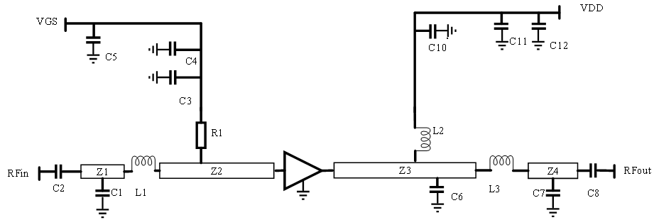
Fig 1. 150MHz Test Circuit
Table 7. List of components
All capacitors should be soldered vertically.
|
Component |
Description |
Value |
Remarks |
|
C1 |
multilayer ceramic chip capacitor |
39 pF |
|
|
C2, C8 |
multilayer ceramic chip capacitor |
680 pF |
|
|
C3,C10 |
multilayer ceramic chip capacitor |
1nF |
|
|
C4 |
multilayer ceramic chip capacitor |
100pF |
|
|
C5 |
multilayer ceramic chip capacitor |
10uF |
|
|
C6 |
multilayer ceramic chip capacitor |
7.5pF |
|
|
C7 |
multilayer ceramic chip capacitor |
24pF |
|
|
C9 |
multilayer ceramic chip capacitor |
18 pF |
|
|
C11 |
multilayer ceramic chip capacitor |
100nF |
|
|
C12 |
multilayer ceramic chip capacitor |
10uF |
Electrolytic capacitor |
|
L1 |
Chip inductor |
68nH |
|
|
L2 |
6 turns enameled copper wire |
D = 0.5 mm; length = 105 mm |
|
|
L3 |
2 turns enameled copper wire |
D = 0.5 mm; length = 10 mm |
|
|
R1 |
chip resistor |
150Ohm |
|
|
Z1 |
Strip line |
(L x W) 6.5mm×2.2mm |
|
|
Z2 |
Strip line |
(L x W) 9.4mm×2.2mm |
|
|
Z3 |
Strip line |
(L x W) 13.5mm×2.2mm |
|
|
Z4 |
Strip line |
(L x W) 6.1mm×1.9mm |
|
|
Printed-Circuit Board (PCB): |
Rogers 4350B; er = 0.030” F/m; height = 1mm; Cu (top/bottom metallization); |
||
Test information
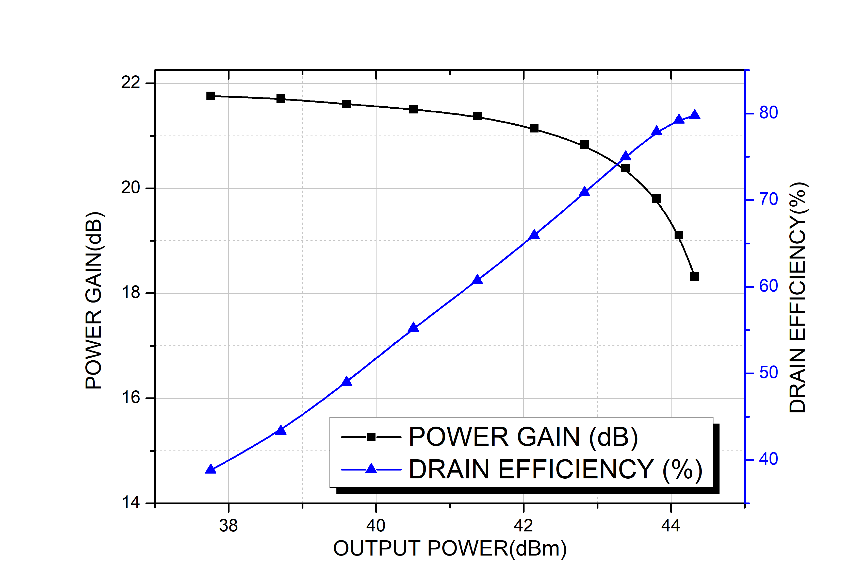
Fig 2. Power Gain and PAE versus Output Power @F=150MHz CW,VDD=28V,IDQ=100mA
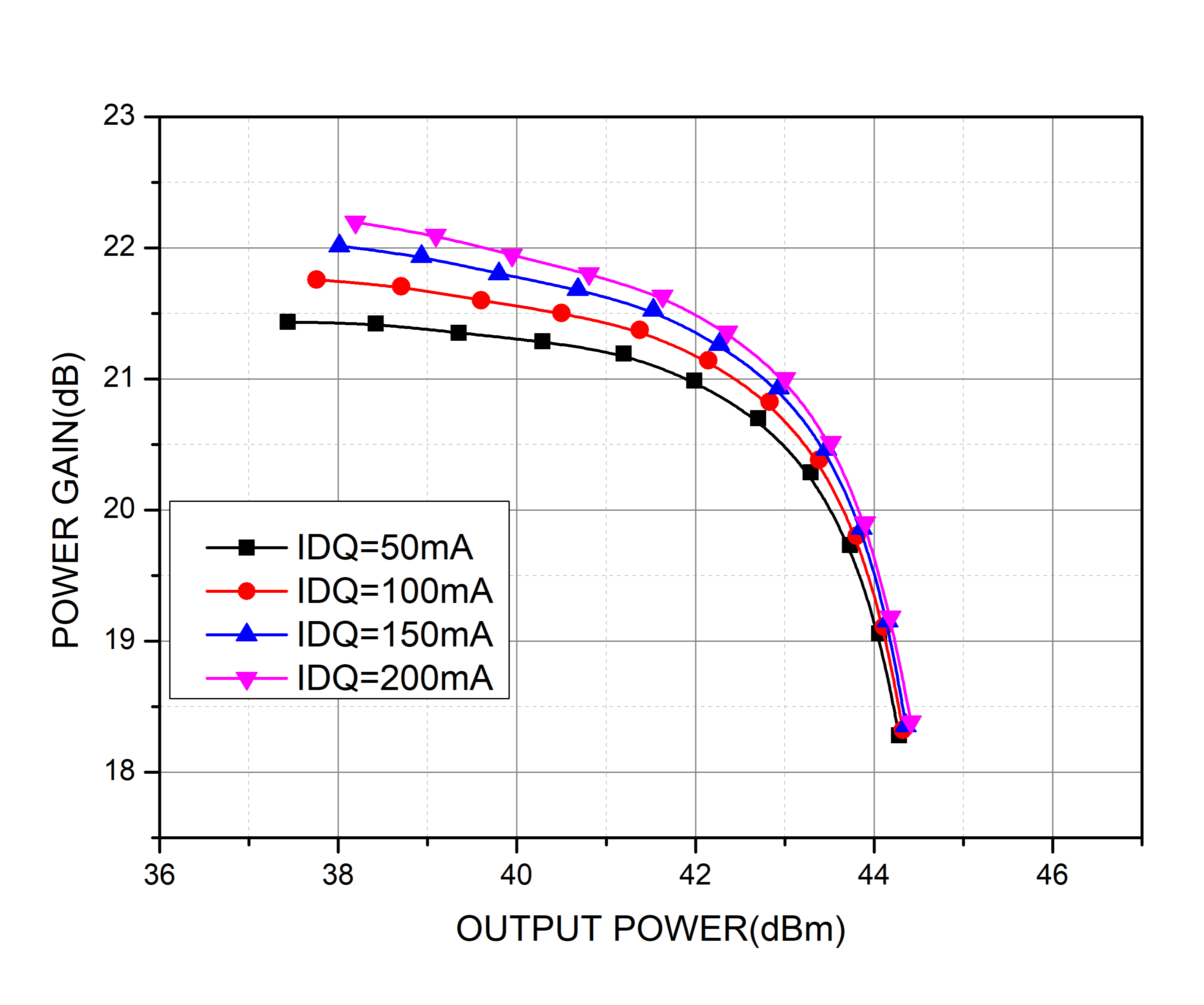
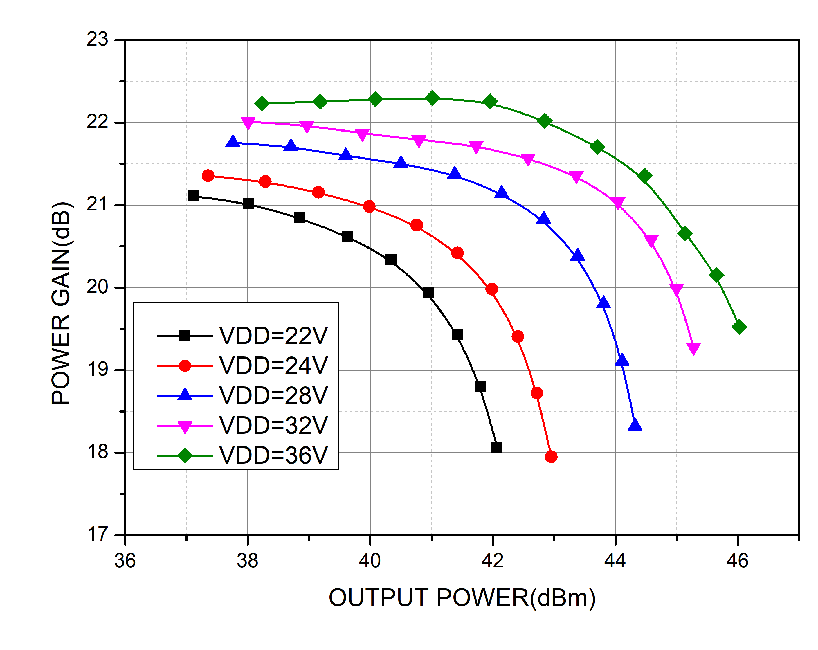
Fig 3. Power Gain versus Output Power
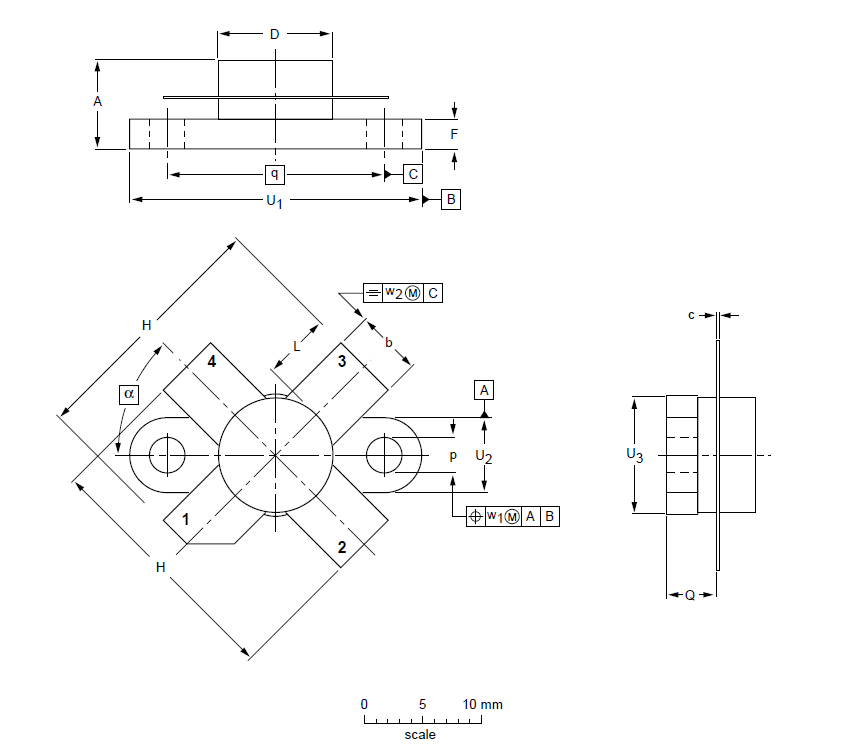
Package outline

Если вам нужна дополнительная информация, пожалуйста, свяжитесь с нами.


